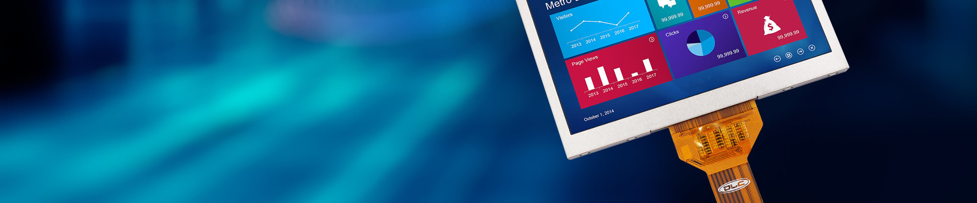

21.5 inch High Brightness IPS TFT Display
• P/N: DLC-T21.5CHL#1
• Size: 21.5 inch
• Resolution: 1920x(RGB)x1080
• Interface: LVDS
• Display Mode: Transmissive Normally Black
• Active Area:476.64 x 268.11mm
• Outline: 495.60 x 292.40 x 10.35mm
• Brightness: 1500cd/m²
• Remarks: High brightness, 50k hours LED life time, Sunlight Readable Display
21.5 inch High Brightness IPS TFT Display
PIN assignment
CN1 (LVDS Interface Signal)
Module Side Connector: UJU IS100-L30O-C23 or Equivalent.
User Side Connector: JAE FI-X30H or Equivalent.
|
Pin No |
Symbol |
Function |
|
1 |
RXO0- |
Negative Transmission data of pixel 0 (ODD) |
|
2 |
RXO0+ |
Positive Transmission data of pixel 0 (ODD) |
|
3 |
RXO1- |
Negative Transmission data of pixel 1 (ODD) |
|
4 |
RXO1+ |
Positive Transmission data of pixel 1 (ODD) |
|
5 |
RXO2- |
Negative Transmission data of pixel 2 (ODD) |
|
6 |
RXO2+ |
Positive Transmission data of pixel 2 (ODD) |
|
7 |
GND |
Power ground |
|
8 |
RXOC- |
Negative Transmission clock (ODD) |
|
9 |
RXOC+ |
Positive Transmission clock (ODD) |
|
10 |
RXO3- |
Negative Transmission data of pixel 3 (ODD) |
|
11 |
RXO3+ |
Positive Transmission data of pixel 3 (ODD) |
|
12 |
RXE0- |
Negative Transmission data of pixel 0 (EVEN) |
|
13 |
RXE0+ |
Positive Transmission data of pixel 0 (EVEN) |
|
14 |
GND |
Power ground |
|
15 |
RXE1- |
Negative Transmission data of pixel 1 (EVEN) |
|
16 |
RXE1+ |
Positive Transmission data of pixel 1 (EVEN) |
|
17 |
GND |
Power ground |
|
18 |
RXE2- |
Negative Transmission data of pixel 2 (EVEN) |
|
19 |
RXE2+ |
Positive Transmission data of pixel 2 (EVEN) |
|
20 |
RXEC- |
Negative Transmission clock (EVEN) |
|
21 |
RXEC+ |
Positive Transmission clock (EVEN) |
|
22 |
RXE3- |
Negative Transmission data of pixel 3 (EVEN) |
|
23 |
RXE3+ |
Positive Transmission data of pixel 3 (EVEN) |
|
24 |
GND |
Power ground Note1 |
|
25 |
NC |
No connection |
|
26 |
NC |
No connection |
|
27 |
NC |
No connection |
|
28 |
VDD |
Power supply: +5V |
|
29 |
VDD |
Power supply: +5V |
|
30 |
VDD |
Power supply: +5V |
Note: This pin should be connected with GND.
CN2 (LED Light Bar)
|
Pin No |
Symbol |
Function |
|
1~5 |
VDDB |
Power supply voltage (+24V) |
|
6~10 |
GND |
Ground |
|
11 |
NC |
No connection |
|
12 |
VBLON |
BL On-Off: High (2.5~5.5V) for BL; Low/Open (0~0.5V) for BL off |
|
13 |
VDIN (Note 1) |
Internal PWM Dimming High (5.5V/100% Duty) for 100% Lum; <NC; when external PWM> |
|
14 |
NC |
No connection |
Note 1: PWM dimming function is included internal PWM and external PWM. Internal PWM: input voltage 0 (GND) ~5.5V to pin 13th, and duty ratio of output voltage/current of inverter is from 30% to 100%. When use pin 13th to control backlight luminance, the pin 14th will be NC.
Environment Conditions
|
Item |
Symbol |
MIN |
MAX |
Unit |
Remark |
|
Operating Temperature |
TOPR |
-20 |
70 |
℃ |
|
|
Storage Temperature |
TSTG |
-30 |
80 |
℃ |
|
Electrical characteristics
|
Item |
Symbol |
MIN |
TYP |
MAX |
Unit |
Remark |
|
Power Supply Voltage |
VDD |
4.5 |
5.0 |
5.5 |
V |
Note1 |
|
Power Supply Current |
IDD |
- |
700 |
1200 |
mA |
|
|
In-Rush Current |
IRUSH |
- |
- |
3.0 |
A |
Note2 |
|
Permissible Input Ripple voltage |
VRF |
- |
- |
300 |
mV |
VDD=5.0V |
|
High level differential input Threshold voltage |
VIH |
- |
- |
+100 |
mV |
|
|
Low level differential input Threshold voltage |
VIL |
-100 |
- |
- |
mV |
|
|
Differential input voltage |
︱VID︱ |
200 |
- |
600 |
mV |
|
|
Differential input common mode voltage |
VCM |
1.0 |
1.2 |
1.5 |
|
VIH =100mV, VIL =100mV |
|
Power Consumption |
PD |
- |
3.5 |
5.4 |
W |
|
Notes:
1. The supply voltage is measured and specified at the interface connector of LCM. The current draw and power consumption specified is for VDD=5.0V, Frame rate=60Hz. Test Pattern of power supply current
- Typ: Color Bar pattern
- Max: Skip subpixe1255
2. Duration of rush current is about 2 ms and rising time of VDD is 520μs ± 20 %
MORE PRODUCTS

undefined
ENQUIRY
Copyright ©DLC Display Co., Limited. All rights reserved.